

AI 3D AOI + SPI,
for PCB Inspection
Horus is the first Physical AI platform designed to begin a new generation of AOI and SPI for SMT productions, with true 3D precision, featuring all possible inspections in the process of PCB assembling with a single platform. Designed to inspect faster, see deeper, and continuously adapt, reducing false positives by a factor of ten and enabling tailored inspections with minimal manual input.

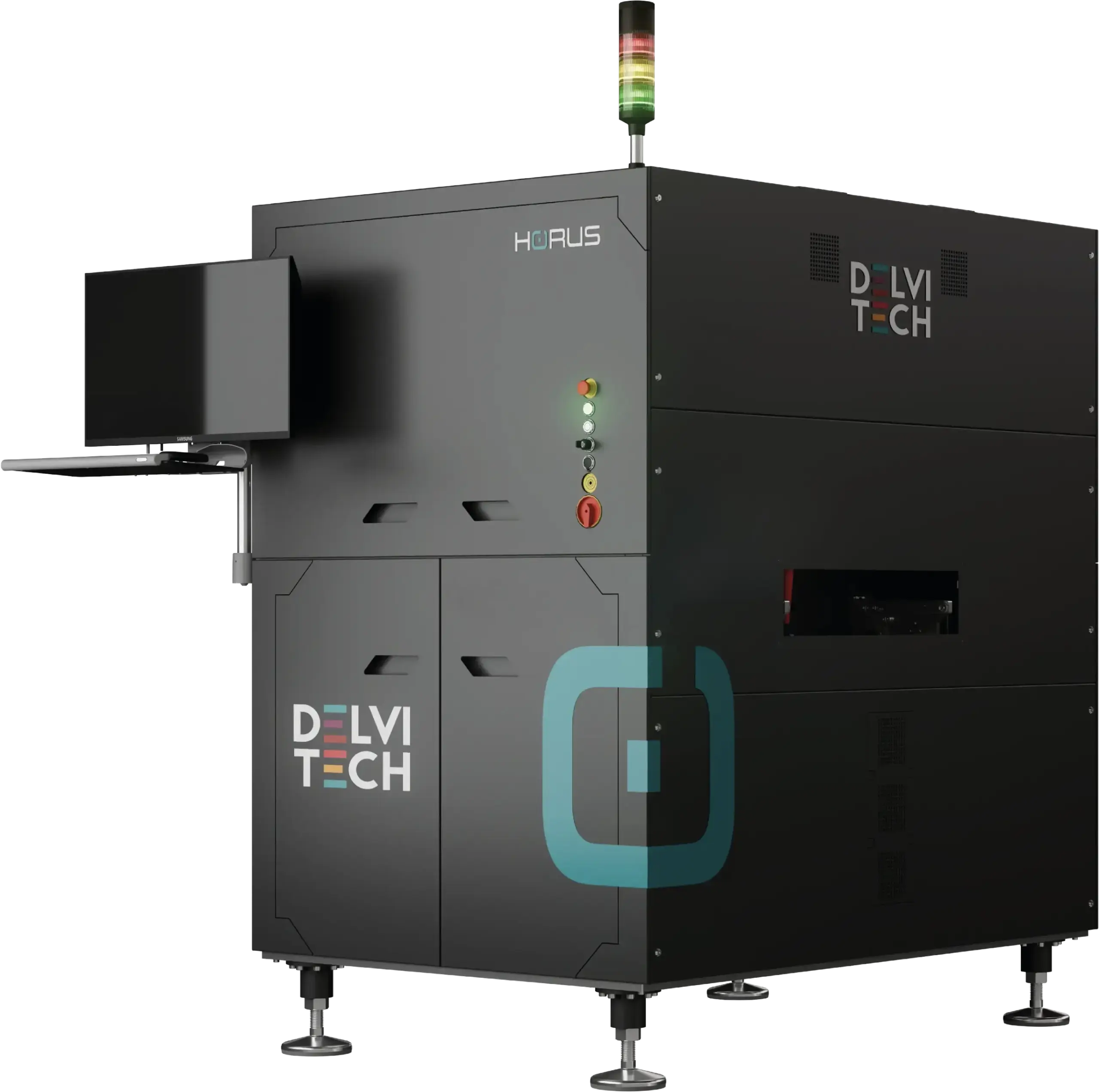
Horus Technical
Specifications.
NEITH Software.
A Unified Platform for Smarter Inspection.
Neith is a web-based software designed for Industry 4.0. It leverages AI to optimize data management, enhance production efficiency, prevent defects and improve first-pass yield. Built on a microservices architecture, Neith offers flexible customization, allowing the integration of personalized inspectors for specific components and ad-hoc interfaces based on existing protocols.
OPTICAL HEAD
Cameras
1 x 25 MP Delvitech high-resolution, high-speed top camera
1 x 12 MP Delvitech polarized camera (optional)
4 x 12 MP Delvitech side cameras (optional)
Projectors
4 x Delvitech full HD RGB projectors for 3D measurements
INSPECTION PERFORMANCE
- Top Camera Resolution 25 MP
- Image Pixel Size 10 µm
- Lens Telecentric
- Field of View Dimensions 50 x 50 mm
- Speed 0.6 sec/FoV
- Lighting Structured RGBW lights + 3 levels LEDs
- Maximum Paste Size 30 mm Height
- Height Resolution 2 µm
- Supported input formats Gerber + CAD, ODB++
- Operating system Windows 11
PCB HANDLING
- Projectors 50 x 50 mm
- Maximum PCB Dimensions 560 x 550 mm
- PCB Thicknesss From 0.5 mm to 5 mm
- Maximum PCB Weight 5 kg
- Minimum Edge Clearance 3 mm
- Top Clearance 60 mm
- Bottom Clearance 60 mm
- Width Adjustment Automatic
- Flow Direction All directions customizable
MACHINE DIMENSIONS & WEIGHT
- Depth 1590 mm
- Height 1791 mm
- Width 1090 mm
- Weight 1170 Kg
One evolving


platform.
Total control for
all PCB Inspection Stages.
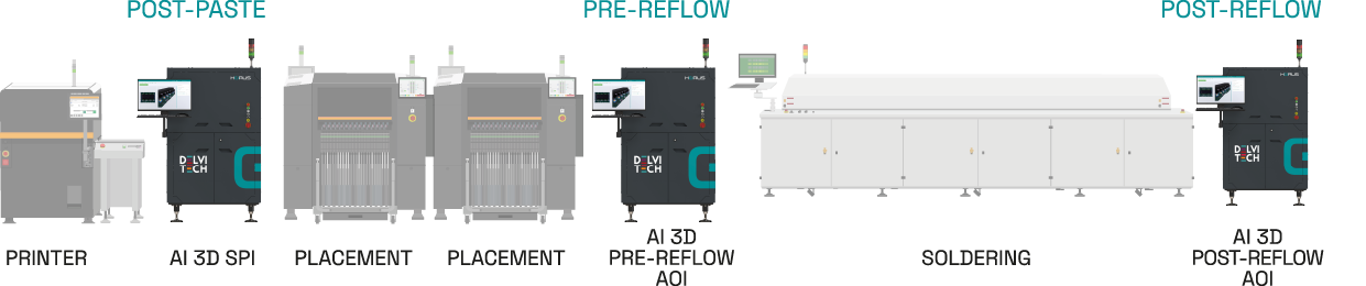
Adaptable across production phases, from Automated Optical Inspection to Solder Paste Inspection, Delvitech empowers engineers with a single, smart inspection program, flexible, scalable, and ready for every production phase. Cloud-enabled and inspection process agnostic, it ensures fast deployment, shared know-how, and reliable results across all facilities.
Download brochure
AOI + AI
- Powered by advanced neural network models for 360-degree inspection coverage
- Component location detection, precise pin contour detection, polarity identification
- Full measurement set: position, height, and volume
- Solder joint analysis (quantitative and qualitative)
- Optical Character Recognition (OCR) capabilities
- Compliance with PCB assembly specifications and IPC classes
SPI + AI
- Detailed inspection of solder paste deposits
- Analysis of location, shape, area, and volume
- Robust bridge detection algorithms
- Dedicated stencil misalignment process inspector
- Real-time feedback to adjust the paste printing process
- Enhances paste application quality and overall production consistency
AOI
SPI
Training
Manager
With Training Manager, your AOI keeps improving without stopping production. Engineers can retrain the neural network directly on the machine, both on line and off line, teaching it new components in real time. The result: fewer errors, higher adaptability, and a system that gets smarter with every shift.
Spot something new
Teach the system
Keep evolving
FAQ
Can Horus perform both AOI and SPI inspections on the same line?


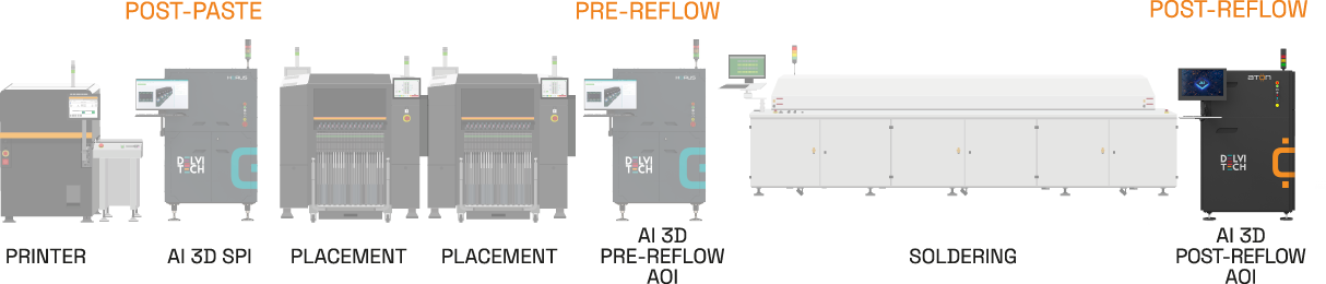
Yes. Horus combines Physical AI 3D AOI + SPI tasks into a single platform, enabling full inspection coverage, from solder paste placement to post-reflow, without additional hardware or separate programming.
Is Horus scalable for high-speed lines or microelectronics?
Absolutely. Horus has a modular architecture thanks to Elements: XP boosts high-speed throughput, HD offers ultra-high resolution for microelectronics, ITU inspects both sides of PCBs, DUO adds dual-lane capability. Delvitech platforms evolves and adapts to your line, not the other way around.
How fast is the Horus inspection process?
Horus processes more than 40 Gbits of data per second and can reach 0.4 sec/FoV with the XP element configuration. Fast PCB management, real-time AI data interpretation, and linear motors ensure industry-leading throughput.
What board sizes and heights can Horus handle?
Horus supports PCBs up to 560 × 550 mm, 5 kg in weight, and 60 mm of top/bottom clearance, making it suitable for tall components, power electronics, and mixed-complexity assemblies.
Is Horus compatible with Industry 4.0 environments?
Yes, Horus is equipped with Neith, a web-based microservices architecture that centralizes all inspection data, can be controlled remotely, even in VR, supports cloud deployment, integrates with MES/ERP systems, and enables custom inspectors and flexible automation. It is therefore designed for complete integration with smart factories.
Can Horus inspect both sides of the PCB?
With the ITU element configuration, Horus rotates PCBs on the X-axis, enabling true 3D inspection on both sides, using a single machine footprint.
How does Horus handle complex or reflective PCB materials?
Delvitech’s patented optical system combines 6 cameras, 4 digital projectors, and RGBW LEDs to capture precise 3D images on reflective metals, dark materials, tall connectors, or shadowed zones.
Can Horus help prevent defects, not just detect them?
Yes. Through predictive algorithms and continuous learning, Horus identifies production deviations early, providing proactive feedback that helps manufacturers eliminate defects before they actually appear on the production line.
AI 3D post-reflow AOI.
Multilevel board inspection up to 140 mm.
Aton is a cutting-edge, Physical AI platform for Automated Optical Inspection, delivering true 3D precision across all post-reflow stages. Designed for maximum adaptability, it ensures reliable inspection even on the most challenging boards, whether large, heavy, densely assembled, or with tall components, helping you maintain quality without compromise.
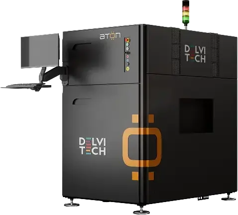
Aton Technical
Specifications.
NEITH Software.
A Unified Platform for Smarter Inspection.
Neith is a web-based software designed for Industry 4.0. It leverages AI to optimize data management, enhance production efficiency, prevent defects and improve first-pass yield. Built on a microservices architecture, Neith offers flexible customization, allowing the integration of personalized inspectors for specific components and ad-hoc interfaces based on existing protocols.
OPTICAL HEAD
Cameras
1 x 25 MP Delvitech high-resolution, high-speed top camera
1 x 12 MP Delvitech polarized camera (optional)
4 x 12 MP Delvitech side cameras (optional)
Projectors
4 x Delvitech full HD RGB projectors for 3D measurements
INSPECTION PERFORMANCE
- Top Camera Resolution 25 MP
- Image Pixel Size 10 µm
- Lens Telecentric
- Field of View Dimensions 50 x 50 mm
- Speed 0.8 sec/FoV
- Lighting Structured RGBW lights + 3 levels LEDs
- Maximum Paste Size 80 mm Height
- Height Resolution 2 µm
- Supported input formats Gerber + CAD, ODB++
- Operating system Windows 11
PCB HANDLING
- Conveyor Z Movement 60 mm
- Minimum PCB Dimensions 50 x 50 mm
- Maximum PCB Dimensions 550 x 500 mm
- PCB Thicknesss ≤ 8 mm
- Maximum PCB Weight 10 kg
- Minimum Edge Clearance 3 mm
- Top Clearance 120 mm
- Bottom Clearance 140 mm
- Width Adjustment Automatic
- Board Warp Compensation ± 5 mm
- Flow Direction All directions customizable
MACHINE MACHINE DIMENSIONS & WEIGHT & WEIGHT
- Depth 1630 mm
- Height 1786 mm
- Width 1140 mm
- Weight 1508 Kg
One powerful
platform.
Complete AI 3D
control for AOI.
Aton is an Physical AI inspection solution that redefines post-reflow AOI with true 3D precision. Engineered to adapt across industries, it handles boards of every size and complexity, even heavy, large, or tall-component assemblies, with outstanding reliability. Equipped with Delvitech's patented 3D optical technology and a six-camera intelligent head, Aton captures crystal-clear data and ensures consistent defect detection. From reflective connectors to fine-pitch components, it delivers the precision and flexibility required for today's most demanding SMT and THT* productions.
Download brochure
AOI + AI
- Powered by advanced neural network models for 360-degree inspection coverage
- Component location detection, precise pin contour detection, polarity identification
- Full measurement set: position, height, and volume
- Solder joint analysis (quantitative and qualitative)
- Optical Character Recognition (OCR) capabilities
- Compliance with PCB assembly specifications and IPC classes
AOI
Training
Manager
With Training Manager, your AOI keeps improving without stopping production. Engineers can retrain the neural network directly on the machine, both on line and off line, teaching it new components in real time. The result: fewer errors, higher adaptability, and a system that gets smarter with every shift.
Spot something new
Teach the system
Keep evolving
FAQ
What makes Aton ideal for inspecting complex, tall-component, or heavy PCBs?
Aton combines true 3D measurement with a Z-axis system, up to 140 mm bottom clearance, and support for boards up to 10 kg. This makes the platform uniquely suit for assemblies where traditional AOI systems struggle, such as with dense, mechanically heavy PCBs with tall connectors.
Can Aton handle large-format PCBs used in industrial or power electronics?
Yes. Aton supports boards up to 550 × 500 mm, ensuring reliable inspection for large-format assemblies commonly used in power electronics, industrial automation, automotive, and energy systems.
How fast is Aton in processing inspection data?
Aton processes up to 40 Gbits of data per second, thanks to FPGA-assisted imaging and linear motor-driven movement. This speed ensures high throughput without compromising accuracy.
Is Aton suitable for both SMT and THT inspections?
Yes, thanks to its up to 140 mm wide bottom clearance, high-definition optics and precise AI models, Aton handles tall pins, connectors, THT solder joints, dense SMT areas and mixed-technology boards with consistent accuracy.
How does Aton maintain accuracy on boards with high solder joint density?
Its true and advanced 3D solder joint analysis technology evaluates quantitative and qualitative parameters, ensuring reliable inspection results even in dense, multi-joint areas.
Is Aton compatible with Industry 4.0 environments?
Yes, Aton is equipped with Neith, a web-based microservices architecture that centralizes all inspection data, can be controlled remotely, including in VR, supports cloud deployment, integrates with MES/ERP systems, and enables flexible automation. It is therefore designed for full integration with smart factories.