
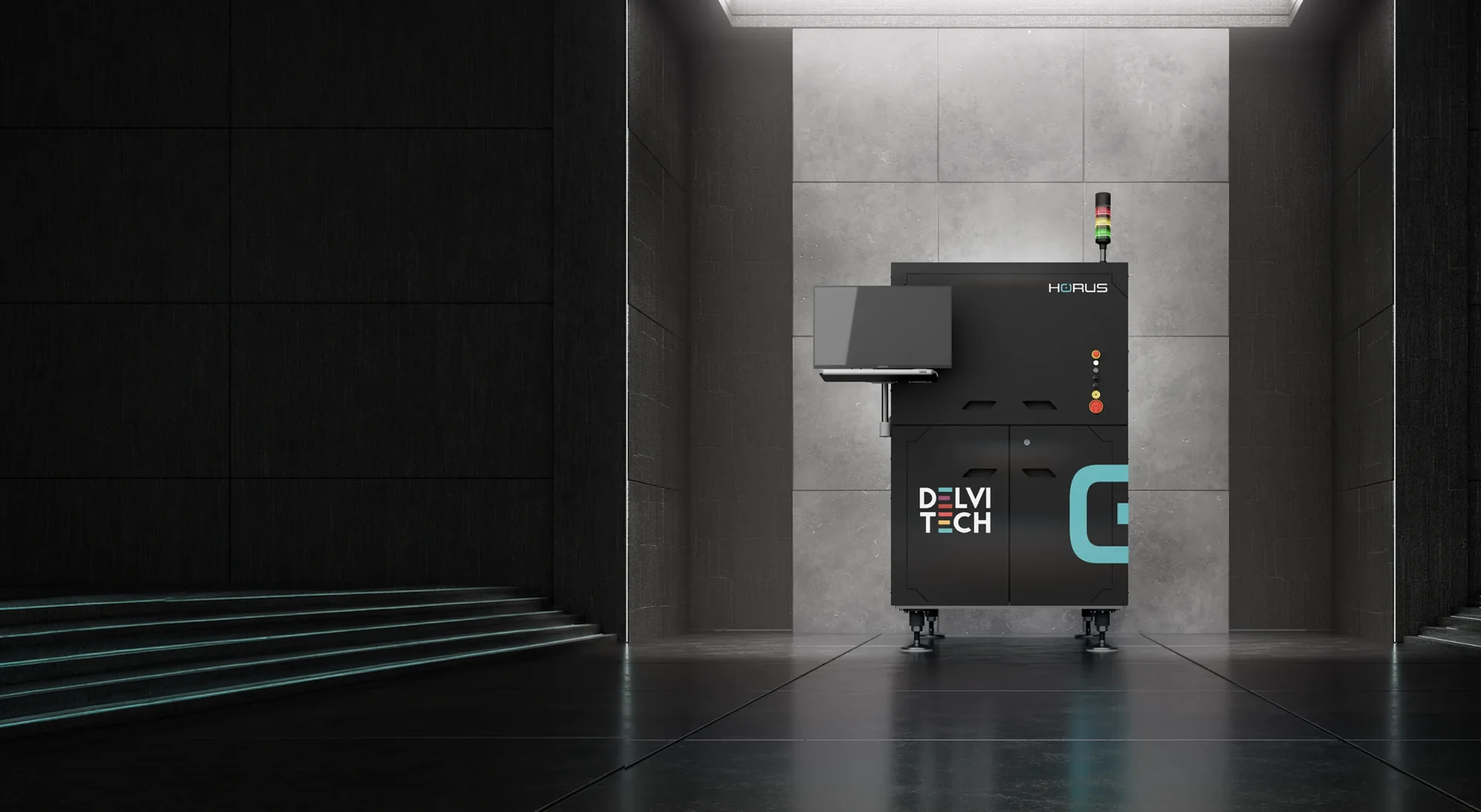
AI 3D AOI + SPI for PCB inspection
Horus
One AI-native platform.
Every PCB inspection stage.
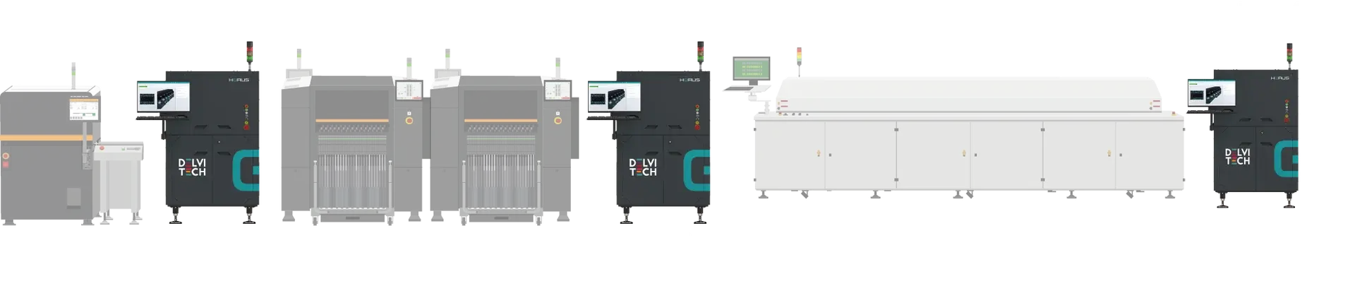
Three inspection stages. One platform. Horus runs 3D solder paste inspection, pre-reflow AOI and post-reflow AOI on the same hardware and the same software. One programming environment, one operator training, one set of spares across the line, and a platform you can reassign to a different stage when production changes.
Horus
Overview Configurations What it inspects Technology Programming
3 stages
SPI · pre-reflow AOI · post-reflow AOI
560 x 550 mm
max. board length x width
0.6 s
per full-3D field of view
60 mm
clearance, top and bottom
25 MP
telecentric imaging
True 3D and high-resolution 2D
multi-level RGBW lighting
Configurations
Configurable by design
Single Lane
The standard Horus.
Boards up to 560 x 550 mm, 0.5 to 5 mm thick and up to 5 kg, with automatic width adjustment and 60 mm clearance above and below. Flow in either direction, to fit any line layout.
ITU (Integrated Tilt Unit)
Both board sides. One platform.
An automatic carrier-flipping system inspects the top and bottom of the board in sequence, inside the same compact Horus. Carrier up to 330 x 340 mm, 3 to 5 mm thick, up to 3 kg.**
Specifications at a glance
| Single Lane | ITU | |
|---|---|---|
| Inspection | 3D SPI · pre-reflow AOI · post-reflow AOI | 3D SPI · pre-reflow AOI · post-reflow AOI |
| Optics | 25 MP top camera, 4 RGB projectors, custom telecentric lens | 25 MP top camera, 4 RGB projectors, custom telecentric lens |
| Field of view | 50 x 50 mm in 0.6 s/FoV | 50 x 50 mm in 0.6 s/FoV |
| Height resolution | 2 µm | 2 µm |
| Height measurement range | Up to 30 mm | Up to 30 mm |
| Max. board (X, Y)* | 560 x 550 mm | 330 x 340 mm carrier |
| Thickness (Min-Max) | 0.5-5 mm | 3-5 mm carrier |
| Max. weight | 5 kg | 3 kg** |
| Clearance top / bottom | 60 / 60 mm · 3 mm edge | 60 / 60 mm · 3 mm edge |
| Machine dimensions (W, D, H) | 1,090 x 1,590 x 1,791 mm | 1,090 x 1,590 x 1,791 mm |
*X=Length, Y=Width. **Preliminary values. Specifications may vary based on system configuration.
What it inspects
Inspect virtually every component
From paste deposit to finished joint, read by neural networks on high-resolution 2D and true-3D data together.
Body and placement
Component location, size and position, tilt and lift, with IPC-oriented acceptance criteria.
Neith readout Locations
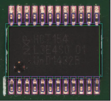
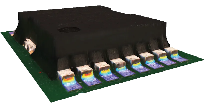
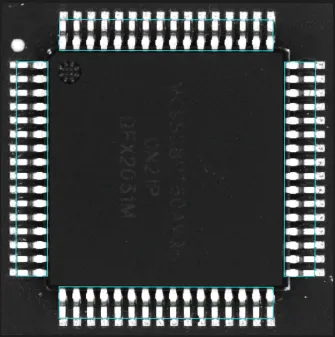
Leads, solder and marking
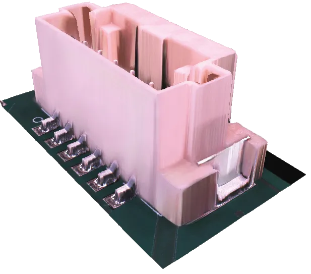
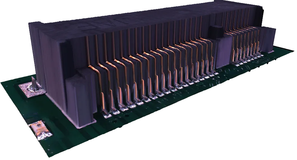
Pin and lead presence and position, solder joint condition, bridges, planarity, solder balls and detection of display scratches, with IPC-oriented acceptance criteria.
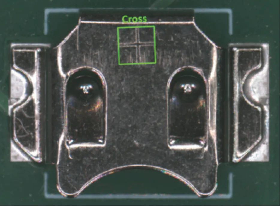
Neith readout Pin solder joint 3D / Tall white connector 3D
Difficult geometries
Reflective surfaces and metallic pins. High-density fine-pitch. Deep shadows and tall connectors. Macro and non-standard applications.
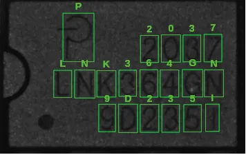
Marking and orientation
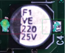
Polarity, OCR and OCV, including rotated text and supplier variants, plus resistor colour-band identification.
Neith readout OCR / Polarity
Beyond the standard inspectors
Macro builds custom tests for geometries no standard inspector covers: heights, distances, coplanarity. Anomaly detection flags deviations nobody wrote a rule for, at component level and across the whole board.
Neith readout Anomaly detector
Step stencils
Automated inspection support.
Deposit consistency
2D/3D comparison across identical components, focusing on height.
Full-board 3D inspection
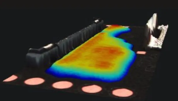
Detect unexpected paste deposits.
Board control
Pass/fail, quality flags, pass-through to AOI and repair-station inspection locks.
Neith readout SOIC smearing / Missing BGA and planarity / QFP peaking planarity
joint 3D
connector 3D
detector
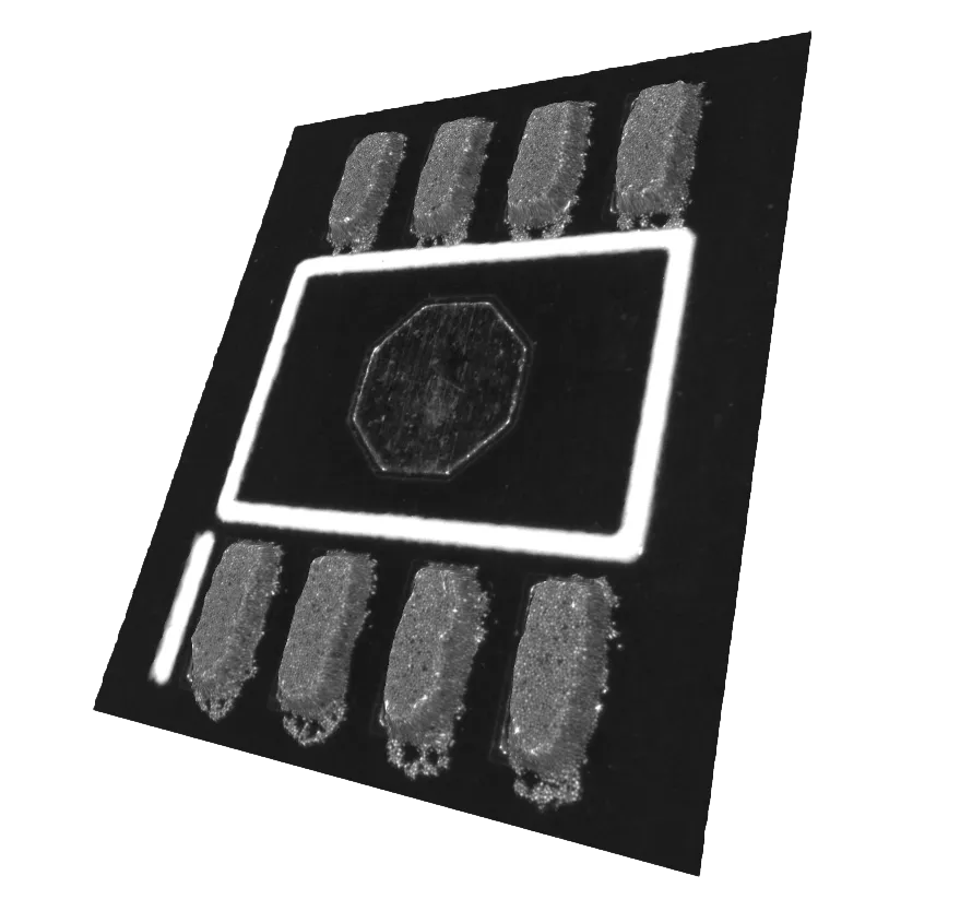
smearing
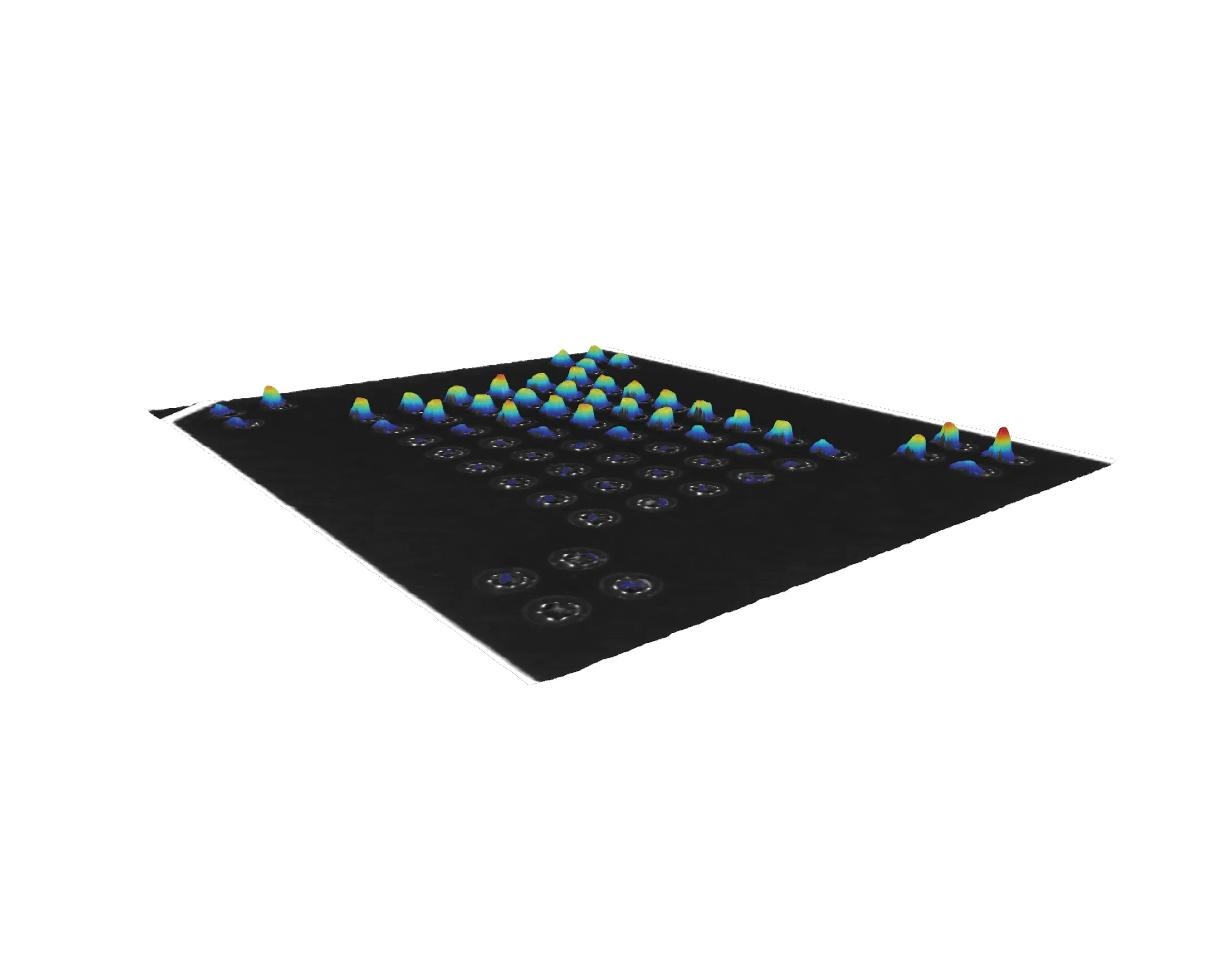
and planarity
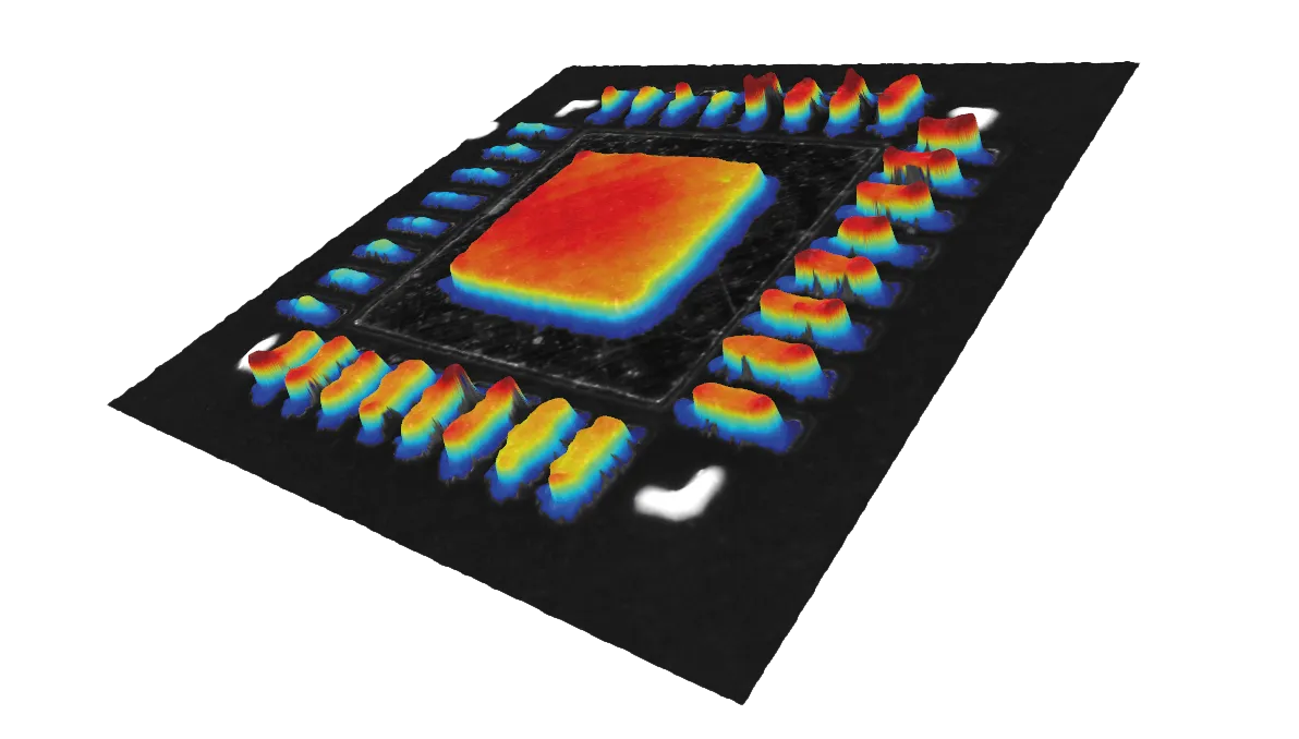
planarity
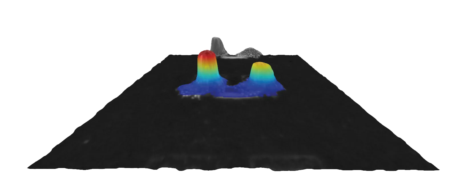
See what others miss
Underfill
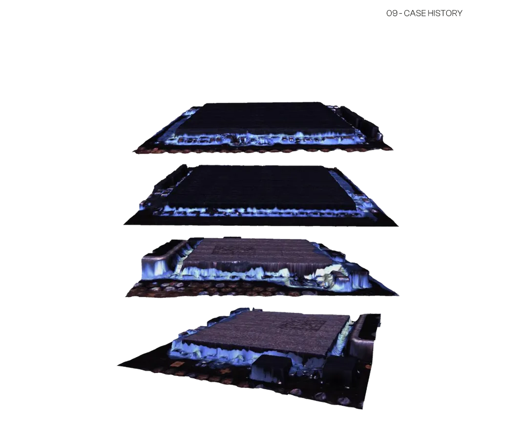
UV-reactive underfill inspected with UV illumination, enabling 3D reconstruction to verify glue presence, distribution and applied amount.
Encapsulation
Encapsulant volume, height and coverage inspected in true 3D, so a component is confirmed protected, not just present.
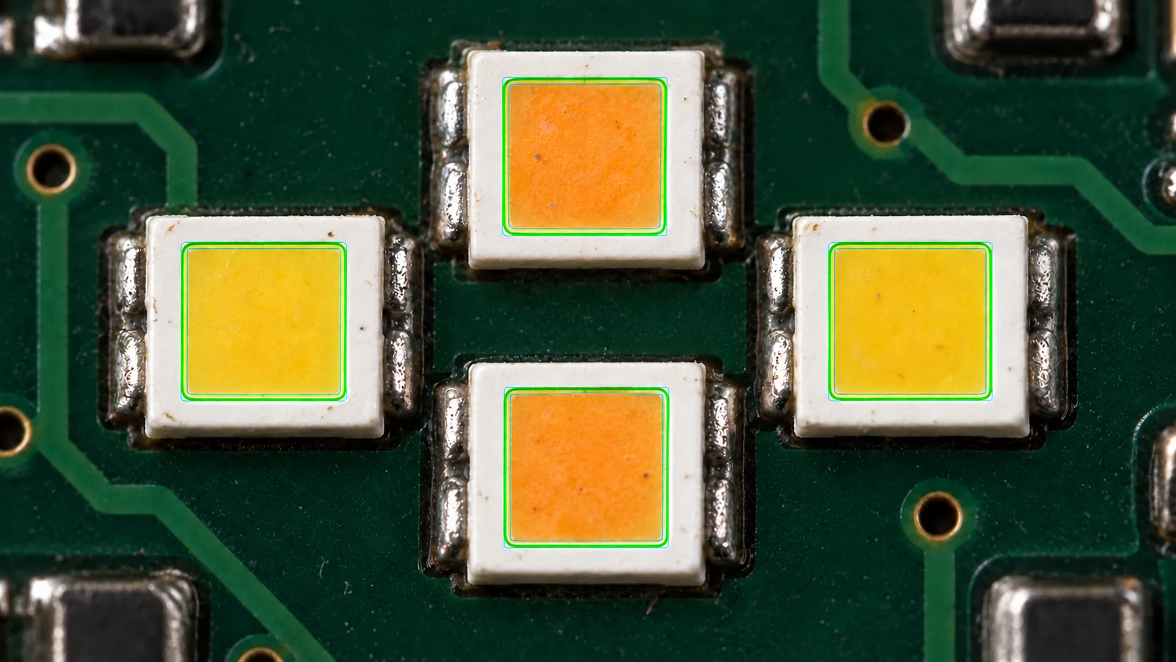
LED
Position, coplanarity and die alignment inspection, even on reflective packages, with reliable identification of the LED’s true colour without interference from die fluorescence.
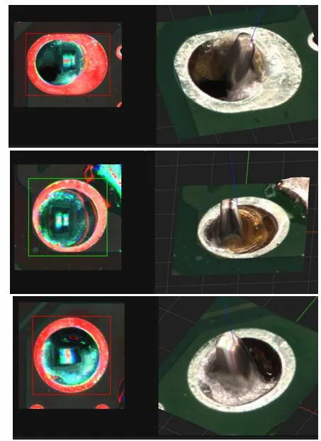
Pin-in-paste
Inspection of through-hole leads inserted into solder paste before reflow, verifying lead position and paste coverage during the same inspection cycle as SMT components.
Send us a difficult assembly.
We run it and send back what the platform has found.
The technology inside
The technology that makes it possible
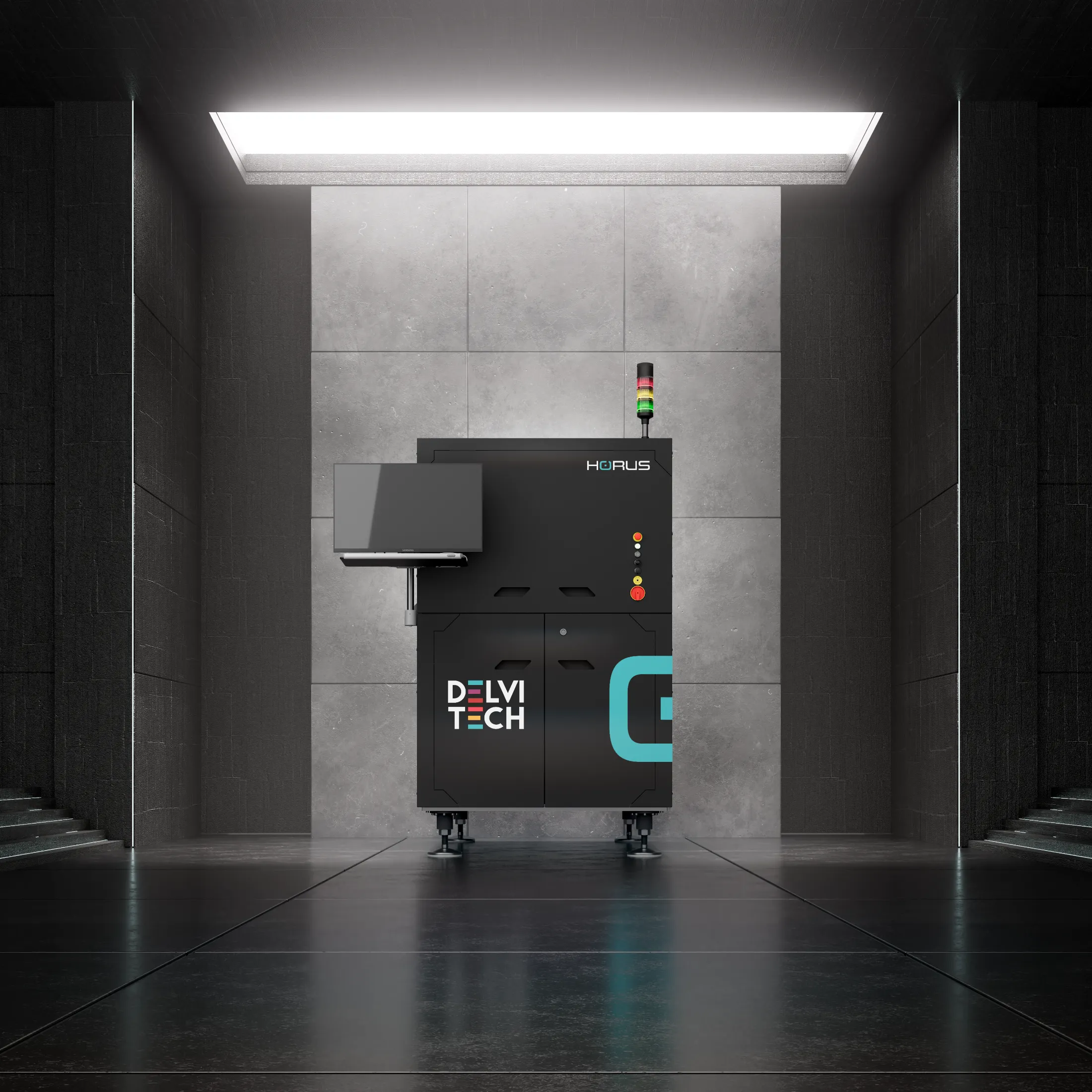
True 3D. Patented optical head.
A 25 MP telecentric top camera, four RGB projectors and multi-level RGBW lighting, with optional polarised and side cameras. Built for reflective metals, shadowed zones, tall connectors and fine pitch.
AI in the Inspection Cycle
It decides during the inspection cycle, not after it. Proprietary neural networks recognise and classify board features in real time, with FPGA processing keeping pace with the line.
Neith Software Platform
One browser-based software environment for programming, data and workflows, across every inspection stage and every Delvitech platform.
Programming and learning
AI Programming and Learning
Training Manager
Your team can train the neural networks directly on the platform, using your own boards and production images. The machine learns to recognise components beyond its initial training while preserving existing knowledge, allowing your team to adapt inspection independently and keep know-how in-house.
Self-programming
Accelerates component recognition and recipe creation, reducing the engineering effort required to bring a new product to stable inspection.
Coming Soon
Predictivity
Proactive process control through neural pattern prediction, recognising what precedes a defect before one occurs.
Coming Soon
Automated Validation Station
The system autonomously analyses components and defects, validates recurring calls and uses AI to optimise inspection parameters, verifying each change against a pass/fail reference set.
Where it fits
Horus is built for most PCBA and electromechanical inspection applications: automotive and EV, Electronics Manufacturing Services (EMS), industrial and power electronics, aerospace and defence, medical devices, telecommunications, AI computing and data centres and consumer electronics, wherever several inspection stages run on one line and the team would rather learn one platform than three.
Brochure
Download the Horus brochure
Enter your email and we will send you a link to download the brochure.
FAQ
Which inspection stages can Horus perform?
Horus performs 3D solder paste inspection (SPI), pre-reflow AOI and post-reflow AOI.
What board sizes can Horus handle?
In the Single Lane configuration, Horus handles boards up to 560 x 550 mm, 0.5 to 5 mm thick and up to 5 kg. The ITU configuration handles carriers up to 330 x 340 mm, 3 to 5 mm thick and up to 3 kg; the page notes that the weight value is preliminary.
What does the ITU configuration do?
ITU uses an automatic carrier-flipping system to inspect the top and bottom of a board in sequence inside the same Horus system.
What can Horus inspect on electronic assemblies?
Horus inspects component placement, leads, solder joints, marking and polarity, as well as difficult geometries such as reflective surfaces, fine-pitch features, deep shadows and tall connectors. Its SPI functions include checking deposit consistency and detecting unexpected paste deposits.
How can a team adapt Horus inspection to its own production images?
With Training Manager, the team can train neural networks on the platform using its own boards and production images. The page says the machine can learn to recognise components beyond its initial training while preserving existing knowledge.

